高通验证首代 HBC 芯片
高通称,其第一代高带宽计算(HBC)芯片已在圣迭戈实验室完成硬件验证,涵盖完整内存读写路径及近存计算。该公司还已完成搭载此架构的数据中心产品流片,首款采用该技术的 Dragonfly AI250 加速器计划于 2027 年上半年送样。高通公布 AI250 的有效内存带宽为 133 TB/s,但与 LPDDR5X 及 HBM4 预计规格的对比属于厂商估算,并非独立基准测试结果。
此次验证和流片是高通解决数据中心 AI 推理中内存带宽与数据搬运瓶颈的一项具体硬件进展。
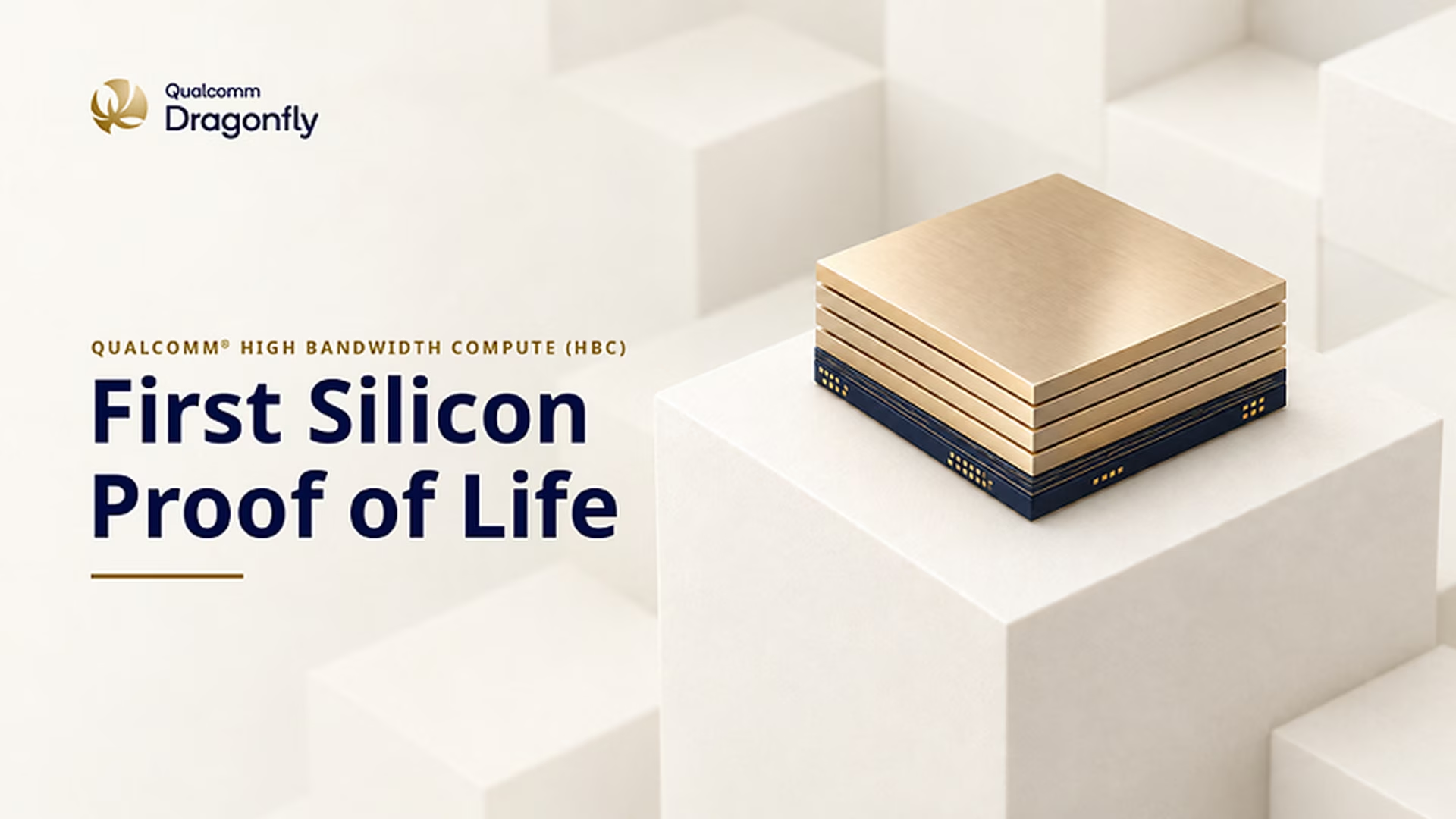

Qualcomm has completed testing the first chips built with its High Bandwidth Compute (HBC) memory technology, clearing a key step towards using it in data centre AI hardware. The company announced the results, saying the technology will feature in its Dragonfly AI250 accelerator, designed to run AI models in data centres.
Best known for its Snapdragon smartphone chips, Qualcomm introduced the Dragonfly brand for its data centre products in June. HBC is designed to address one of the main bottlenecks in running large language models at scale: moving data quickly enough between memory and processors.
#Qualcomm#Dragonfly AI250#High Bandwidth Compute#Dragonfly Rack#Dragonfly AI200#Dragonfly AI300#LPDDR5X#HBM4