Samsung Expands Advanced Packaging R&D in Yokohama
Samsung Electronics chairman Lee Jae-yong visited Samsung's Advanced Package Lab in Yokohama on November 1 to review next-generation semiconductor packaging research and discuss cooperation with Japan's materials, components and equipment industries. Samsung says the lab was established in 2023, formally opened in September 2026, and will expand research into wafer bonding, glass substrates and production-ready packaging architectures. The company also plans to invest ¥40 billion over five years from 2024 to build its Japanese research base.
The visit and reported expansion connect advanced-packaging development, including materials and process technologies, with Samsung's AI-chip strategy and Japan's semiconductor supply chain.
李在鎔視察三星橫濱先進封裝實驗室,強化日本材料與設備供應鏈合作 | TechNews 科技新報

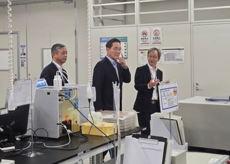
三星電子(Samsung Electronics)會長李在鎔(Lee Jae-yong)於 11 月 1 日造訪位於日本橫濱的先進封裝實驗室(APL),親自了解次世代半導體封裝技術的研發進度,並與研究人員討論如何進一步強化與日本材料、零組件與設備產業的合作。
三星表示,李在鎔此行的重點在於先進封裝材料與製程技術的開發狀況。由於先進封裝已成為提升 AI 晶片效能與維持半導體競爭力的核心環節,他也強調必須持續掌握相關技術,才能在 AI 時代維持優勢。
#Samsung Electronics#Samsung Advanced Package Lab#Lee Jae-yong