Taiwan SiC makers push toward 12-inch wafers for AI power and packaging
TechNews reports that Taiwanese silicon-carbide materials suppliers are advancing larger-diameter wafers and expanding into AI thermal and advanced-packaging applications. Shengxin Materials said it has completed growth of a 12-inch SiC single-crystal ingot using in-house equipment and processes, while noting that 12-inch material remains in technical development and still needs process and application validation. Paragon's subsidiary Crystal Cheng has finished its Chiayi 8-inch SiC substrate plant, targeted for full production in Q1 2027, with 8-inch conductive-type substrates already shipping in small volumes; GlobalWafers chair Doris Hsu said the company will prioritize high-thermal-conductivity 12-inch SiC wafers. The report notes that moving from 8-inch to 12-inch still faces crystal-defect, thermal-stress, processing and cost challenges.
The report says SiC is seen as a candidate material for high-voltage power conversion and chip heat spreading as AI data centers move to high-voltage DC distribution and GPU and HBM power density rises.

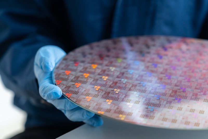
隨 AI 電源及高頻通訊需求持續發展,台灣碳化矽(SiC)材料業者加速推進大尺寸晶圓技術,並逐步拓展 AI 散熱與先進封裝等新興應用。其中,盛新材料已完成 12 吋 SiC 單晶晶錠長晶,柏騰旗下晶成材料推進 8 吋 SiC 基板量產,中美晶旗下環球晶則將高熱傳導係數的 12 吋 SiC 晶圓列為研發重點。
盛新材料昨(12)日舉行興櫃前法人說明會。除了既有 6 吋及 8 吋 SiC 產品,公司也透過自主研發設備及製程技術,成功完成 12 吋 SiC 單晶晶錠長晶,未來將進一步拓展散熱、先進封裝及光學材料等應用。公司表示,12 吋材料仍處於技術開發階段,後續將持續推進相關製程與應用驗證。