Samsung reportedly targets early 2027 for 3D Cube-H development
IT之家, citing ZDNET Korea, and TechNews report that Samsung Electronics plans to complete development of its hybrid-bonded 3D Cube-H advanced packaging by early 2027. The technology targets ultra-high-performance AI chips and is reported to offer about 6 μm terminal pitch, with possible GPU or logic-on-HBM stacking architectures. The performance, energy-efficiency and thermal claims come from unnamed industry sources and lack independent measurements.
3D Cube-H could expand Samsung’s advanced-packaging offering for high-performance AI semiconductors, but the reported timetable, specifications and customer-evaluation plan remain unconfirmed.

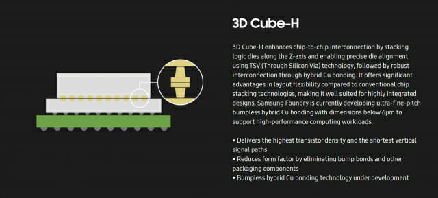
韓國媒體報導,三星電子已確立研發計畫,預計將於 2027 年初完成先進封裝技術「3D Cube-H」的開發。該技術採用混合鍵合(Hybrid Bonding)技術達到垂直(3D)堆疊結構,主要鎖定超高效能人工智慧(AI)半導體應用。業界預期,這項技術若順利推進,將為三星未來在晶圓代工業務爭取各大科技客戶奠定重要基石。
「3D Cube」是三星將多個晶片進行垂直堆疊的先進封裝技術,相較於傳統水平排列結構,能在相同面積內大幅提高電晶體集聚度。三星先前已推出基於熱壓(TC)鍵合技術的「3D Cube-T」。TC 鍵合是在晶片之間加入微型凸塊(Bump),再透過熱與壓力完成接合,技術相對成熟且兼具良率與成本效益。
#Samsung Electronics#Samsung 3D Cube-H#Samsung 3D Cube-T#HBM